Key Features of OHC15L™
– 150nm SiCMOS technology
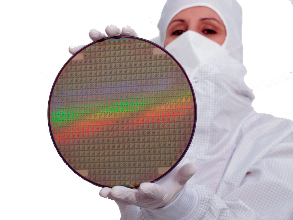
– 8” wafer
– 6 metal / 1 poly
– Isolated wells
– Core voltage 1.8V
– Analog voltages up to 12V
– Clock speed >1GHz
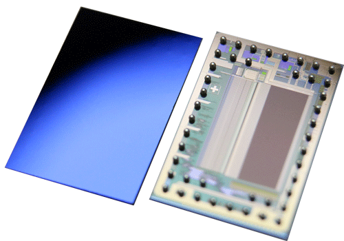
– Backside illumination
– Virtual backside contact
– Active circuits under solder balls (pads)
– Cost effective CSP packaging
The Unique and Flexible Pixel Design
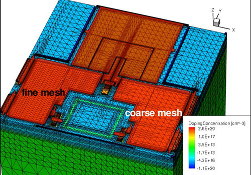
TCAD Flow Simulation
3D Electrical Simulation
Typically, applications need a highly specific and customized pixel design to achieve the required performance. In-pixel charge storage gates, also called frame buffers, are CCD devices which allow signal processing in the charge domain. The technology allows addition and subtraction of charge without adding noise to the signal. It also allows to store hundreds of frames at a frame rate in the tens of millions per second (Mfps) or even higher.
The ESPROS own IP
The design toolbox of ESPROS consists of many already designed and in-use IP. They allow a low risk but high design speed implementation of new ASICs. The toolbox consists, among others:
– Photo diodes
– CCD
– 3D TOF pixels
– LiDAR pixels
– CDS
– Amps
– Comparators
– References
– Regulators
– Charge pumps
– Sources
– Temperature sensors
– ADC, DAC
– LED and LD drivers
– Oscillators
– PLL, DLL
– Digital I/O
– I2C, SPI, LVDS, TCMI
– EEPROM
– Many more