General
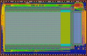
Design projects are based on our OHC15L Silicon CMOS technology for high performance imagers, or on our OHD50L technology node for high performance photo diode and photo diode arrays. Typically, using these technologies will far outperform photonics chips based on standard imaging CMOS processes, due to the very high NIR quantum efficiency of more than 70% @905nm and the high performance CCD, with clock speed up to 250MHz. Completely new implementations are possible, e.g. imagers with a speed of millons of frames per second. We make the unthinkable possible!
Design flow
Typically, the design of an imager with our technology starts with a pixel design by us, if there is no pixel with the specific requirements already available. Our pixel design team uses 3D TCAD software from Synaptics®, with an ESPROS-specific extension, to develop and simulate photonics features.
The chip design process of the electronic circuitry is a standard mixed-signal design flow on a 150nm node, with 1P6M and MIM cap on metal 5. Due to the high resistive base silicon material and STI, isolated devices are available. Thus, multiple voltage domains on one substrate from -15 to +12V are possible.
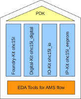
PDK and available IP
The basis is a PDK for the Cadence® design suite containing all necessary devices from 1.8V to 12V transistors, diodes, photo diodes, etc. It also contains a digital library and an I/O library.
An extensive IP library is available to speedup the design of a new chip. Among others, photo diodes, photo gates (CCD), high gain floating diffusion, CDS, CCD driver, TDI imager, TOF pixel (cwTOF & pTOF), in-pixel frame store buffer, voltage and current references, amplifiers, comparators, SAR and flash ADC, DAC, SPI, I2C, LVDS, EEPROM, charge pumps, oscillators, PLL, DLL, temperature sensors, etc.
The existing IP can be used for free in chip design on OHC15L.