Design house
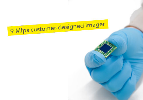
As a design center with several years of imager design experience on our OHC15L™ process, we offer the design of your imager ASIC with shortest possible design time and lowest risk implementation. We understand our customers requirements very well due to our ability to implement complete camera systems with lens, illumination, camera electronics and camera firmware. Many implemented applications are the proof of our competence.
Foundry
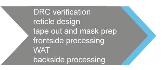
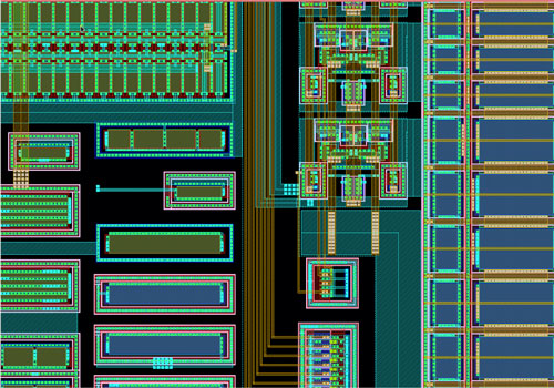
We offer our PDK for Cadence® tools to customers who would like to design their own imager themselves. Typically, ESPROS designs the pixel and its global architecture and the customer implements the other circuitry. We accept GDS-II data where we do DRC. Mask making and production run comletion of successful checks. The customer gets, dependent on the agreement, untested wafers with WAT data, tested dies or even chips on carriers.
IDM
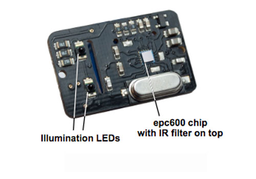
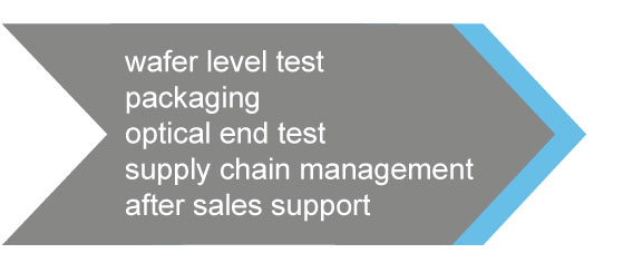
Imagers using the properties of our OHC15L™ technology are typically ultra high speed, e.g. LiDAR chips. They are also quite large, the electrical currents are high and, together with the backside imaging concept, reliable packaging solutions are crucial. Typically, the imagers require bandpass or other optical filters that are part of the package. We offer fully optically tested imagers on carriers which are on qualified packages according AEC-Q100 and JEDEC standards.